.Adopts non-contact measurement technology, without damaging the surface of the object.
.Combined with a high-precision motion control platform, customers can use point/line/area measurement methods for product 3D data analysis as needed.
.Measurement point distance (Resolution) and quantity can be programmatically controlled, without being limited by the hardware constraints of 3D surface scanning
.Applicable to a wide range of products, suitable for all products except for absorbent materials.
.Solutions for 4/6/8-inch wafers
.Highly stable and precise 3D morphology measurement technology
.Multi-functional algorithms for TTV/LTV/BOW/Warp/Thickness
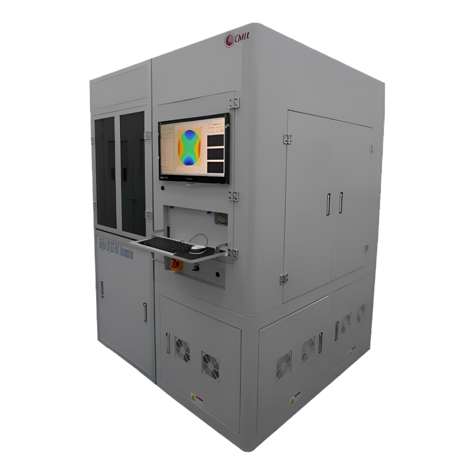
.Convenient operation with diverse engineering analysis and visualized morphology maps(height map, virtual plane height map, contour map, 3D morphology map)
.Block gauge automatic calibration system
.Customized report output
.Automatic sorting system
.Continuous loading and unloading production
| SiC | GaN | GaAs | Silicon | Sapphire |
| v | v | v | v | v |
| Please contact us for further information, as it can be applied to various materials | ||||
| 4″ | 6″ | 8″ |
| v | v | v |