Process

SiC Process

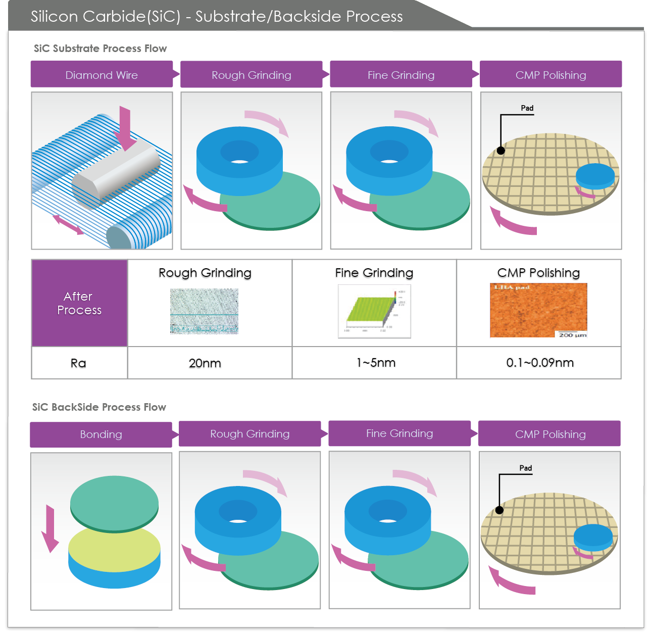
Silicon Carbide (SiC) boasts excellent material characteristics, including wide bandgap semiconductor properties, low conduction losses, high breakdown voltage, and high switching frequency capabilities.

In recent years, SiC has gradually made its way into high-tech fields such as aerospace exploration, telecommunications base stations, automotive engines, and high-frequency devices. It has the potential to become a key driving force in future market product development.

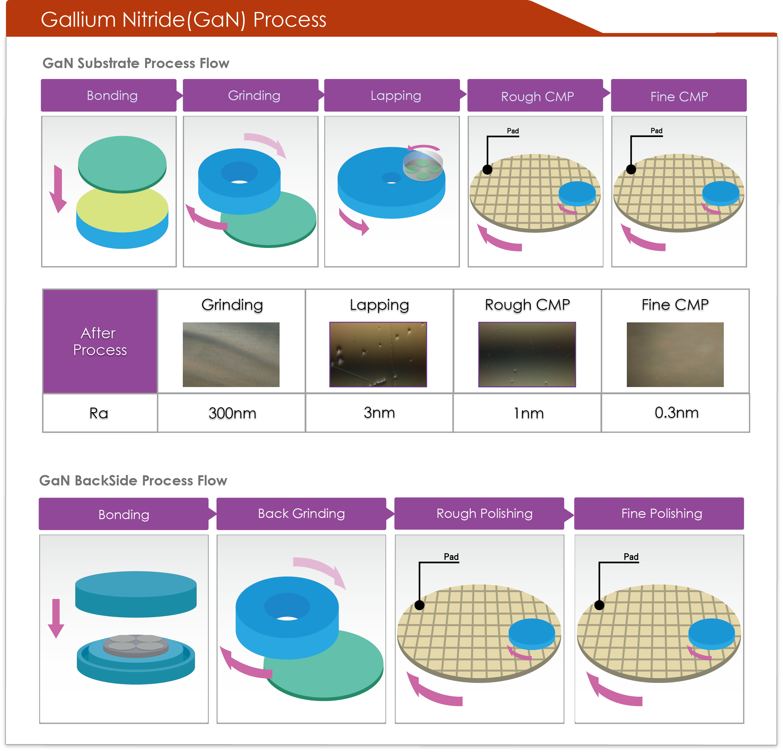
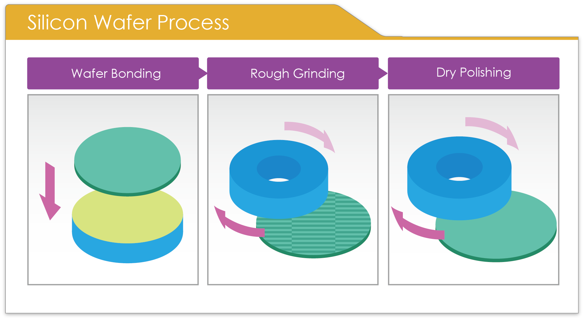
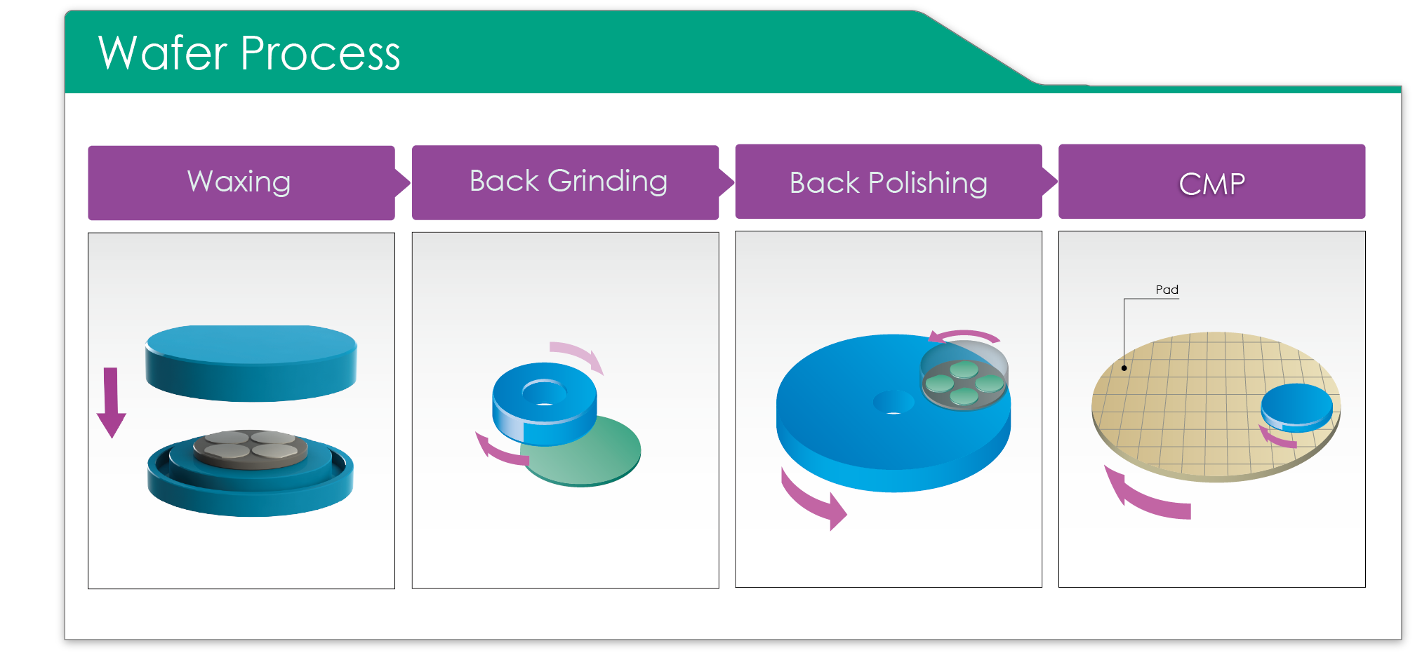
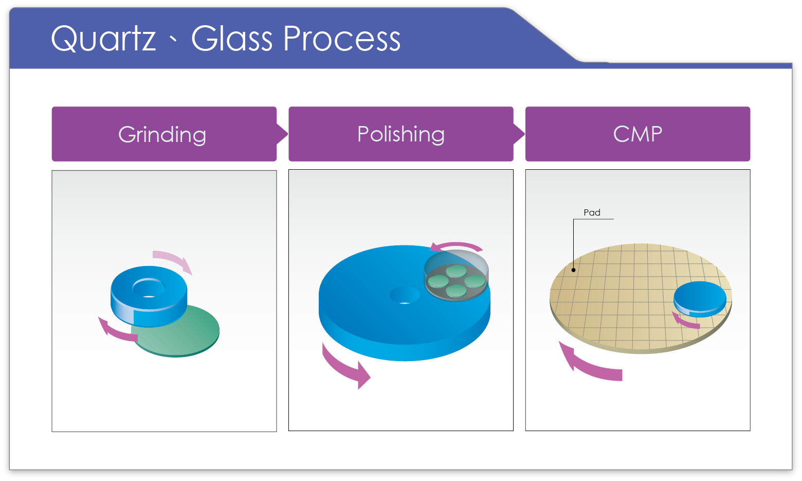
We currently offer materials and processing equipment for cutting, grinding, and polishing, and we also provide contract manufacturing services. We actively engage in new material development in collaboration with strategic partners. Through systematic technological integration, we strive to continuously provide new process technologies and applications for new products. Our goal is to become a competitive and forward-looking industry leader.

GaN Process

Gallium Nitride (GaN) possesses similar material characteristics to Silicon Carbide (SiC), such as wide bandgap semiconductor properties, low conduction losses, high breakdown voltage, and high switching frequency advantages. In specialized application fields, GaN has gradually competed with SiC in the high-tech market and has the potential to become a future product development contender. Emphasizing collaboration with strategic partners, we also value the application of GaN in emerging high-tech markets, actively seeking opportunities to capture larger market prospects in special high-end applications.

We currently offer materials and processing equipment for grinding and polishing, as well as providing contract manufacturing services. We actively engage in new material development with strategic partners, aiming to become a leading industry pioneer in forward-looking technologies.

Silicon Wafer Process

We are actively developing technologies to address the characteristics of Silicon wafers / GaAs, especially for the integration of VCSELs in optical communication applications and 3D sensing applications, to meet the market demand for new products. By combining new process technologies and human resources, we are developing advanced processes and leading industry technologies for the mass production of grinding and polishing of various materials for semiconductors

Sapphire Process

Sapphire is widely used in LED lighting and display applications, and has been expanding with the market expansion in smart terminals in recent years.

In response to the industry's demand, Sapphire has launched a substrate process covering waxing, grinding, polishing, and wafer thinning processes.

In the substrate manufacturing process, Sapphire has advocated innovative processes to the industry, while the wafer backside thinning process is once again an industry-leading process with Kellogg's machines and consumables to effectively increase customer productivity and significantly reduce production costs.

Quartz, Glass Process

In the process of quartz and glass fabrication, polishing is carried out to achieve a smooth and glossy surface that meets specific application requirements. This process involves cleaning, grinding, fine grinding, polishing, cleaning, and inspection, utilizing abrasives, tools, and polishing agents to carefully treat the surface of quartz materials, ensuring high-quality surface precision and flatness. Polishing of quartz plays a crucial role in fields such as optical devices, fiber optic communication, and semiconductor manufacturing, ensuring smoothness and excellent optical performance of the material surface.